Laboratory Overview
Established in December 2025 with the approval of the Beijing Municipal Science and Technology Commission, the Beijing Key Laboratory of Atomic-Scale Precision Manufacturing and Cross-Scale Device Fabrication is dedicated to addressing fundamental scientific challenges and engineering requirements in atomic-scale manufacturing. Its research focuses on precision atomic-scale manipulation and cross-scale synergistic manufacturing, supporting key industrial fields including advanced-node integrated circuits, high-end chips, and emerging semiconductor devices. The Laboratory has strategically prioritized atomic-scale design and simulation, sub-atomic fundamental materials and device fabrication, precision planarization and interface engineering, in-situ measurement and high-resolution characterization techniques, as well as advanced equipment and system integration. By overcoming bottlenecks in large-scale manufacturing and process uniformity control, the Laboratory aims to build a comprehensive innovation ecosystem encompassing fundamental research, technology development, transfer, and industrial application.
Faculty & Researchers
Professor Guoxin Xie serves as the Laboratory Director, with academic directions spearheaded by Professor Jianbin Luo in fundamental atomic-scale manufacturing research and Professor Xinchun Lu in instrumentation and industrial applications. Currently, the Laboratory boasts a dedicated team of 40 researchers, including 1 Member of the Chinese Academy of Sciences, 8 National High-Level Talents (comprising Distinguished Young Scholars, Cheung Kong Scholars, and awardees of the 10000 Talents Program), and 11 key junior faculty members. The Laboratory features a multidisciplinary cohort spanning mechanical engineering, materials science, physics, chemistry, and instrumentation, with over 70% of the faculty holding senior professional ranks. This profound interdisciplinary synergy supports an integrated research and development (R&D) workflow, enabling collaborative innovation from fundamental design and materials development to device fabrication and high-end instrumentation, thereby transforming basic science into industrial-scale engineering solutions.
Research Directions
To address the critical bottlenecks in precise interfacial modulation, scaling-up consistency, and industrial-scale implementation, the Laboratory pursues a synergistic research layout centered on foundational theories, core fabrication techniques, and advanced equipment, encompassing:
nMethodologies and Design in Atomic-Scale Manufacturing: Simulation fidelity and computational scale are often conflicting requirements in atomic-scale modeling, making it challenging to strike a balance between them. To address this challenge, the Laboratory leverages first-principles and multiscale modeling to investigate the evolution of physical properties in atoms and sub-atomic constituents under mechanical, thermal, and electrical stimuli, aiming to elucidate the mechanisms of external fields modulation and defect engineering. In addition, the Laboratory is developing an interfacial database and a high-throughput computing platform, leveraging artificial intelligence (AI)-driven informatics to enable predictive modeling of interface characteristics while optimizing both structural and processing parameters.
nAtomic-Scale Material Synthesis and Device Fabrication: To address the challenges in constituent material preparation and device fabrication, the Laboratory conducts systematic research into controllable material synthesis, defect modulation, and stable dispersion, facilitating the development of cross-scale assembly and arraying technologies. Through breakthroughs in mastering the precision atomic kinetics governing confined adsorption, migration, and rearrangement, the Laboratory enables ordered atomic-level structuring, providing the technical support for the innovation of next-generation high-performance devices.
nAtomic-Scale Processing Technologies and Equipment: To meet the demands for atomic precision removal and damage-free machining of heterogeneous materials, the Laboratory’s research focuses on mechanisms of atomic-scale removal and interfacial evolution driven by multi-physical fields coupling, aiming for novel processing technologies. Furthermore, by advancing the synergistic design of processes and equipment, the Laboratory seeks to break through critical technologies in equipment R&D, ensuring reliable atomic-precision production for large-scale applications.
nAtomic-Scale Metrology and Characterization: To address the requirements for high-precision detection in atomic-scale manufacturing, the Laboratory develops in-situ characterization techniques with high temporal and spatial resolution to investigate the formation and evolution mechanisms of surface defects. Moreover, the Laboratory aims to establish online detection methodologies for identifying types and densities of atomic-level defects, enabling the precise characterization and dynamic monitoring of their structural features and interfacial behaviors.
Research Achievements
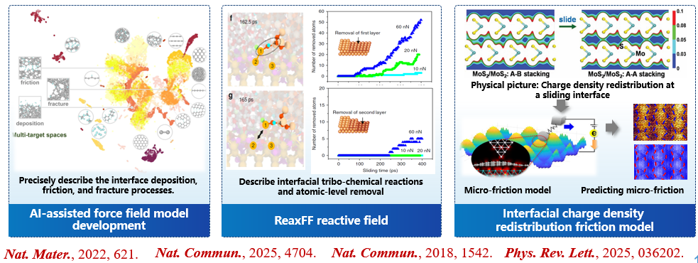
■Research Achievement 1: An AI-assisted force field model and reaction force field were established, with results published in journals such as Nat. Mater. and Nat. Commun., and awarded the Second Prize of the National Natural Science Award in 2018.
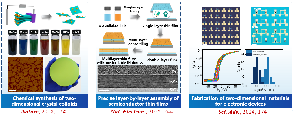
■Research Achievement 2: A new chemical synthesis route for high-purity ultrathin two-dimensional material colloidal solutions was proposed, achieving improvements in energy levels such as carrier mobility, with results published in journals such as Nature and Nat. Electron..
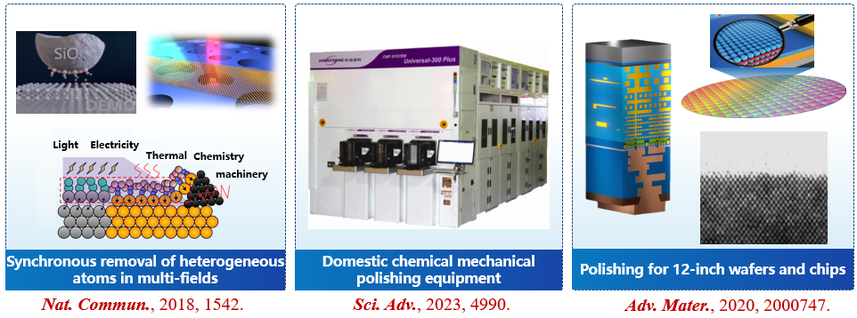
■Research Achievement 3: A systematic chemical mechanical polishing equipment was developed, with over 700 sets applied in production lines at companies such as Semiconductor Manufacturing International Corporation (SMIC), achieving a domestic market share of >60%, and was awarded the First Prize of the National Technological Invention Award and the Special Prize of the Machinery Industry Award in 2023.
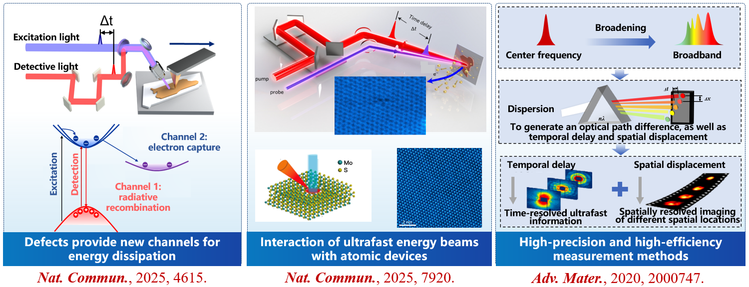
■Research Achievement 4: An atomic-level defect detection technology for material interfaces based on the ultrafast electron energy dissipation mechanism was proposed, awarding the First Prize of the Tianjin Technological Invention Award in 2024, the Second Prize of the Beijing Natural Science Award in 2023, and the China Patent Silver Award.